
Packaging
Ceramic, plastic and specialist package configurations for obsolete semiconductor replacements
Packaging is often where replacement strategies can fail. Matching electrical performance alone is not sufficient if the device cannot integrate into the existing system or perform as required in its operating environment. This is why package selection is a key part of an obsolescence solution.
Force Technologies supports a wide range of package options, but the focus is always on what will actually work in application. In practice that means looking at how the device needs to fit within the existing design, how it will perform electrically and thermally, and whether it can handle the environmental conditions it will be exposed to over time.
In some cases, that will be a direct like-for-like package. In others, a different approach may be more suitable to maintain performance and long-term reliability while still supporting continuity.
The aim is simple: to provide a replacement device that fits as expected, performs as required, and doesn’t introduce additional engineering challenges.
Force Technologies offers an extensive range of ceramic and plastic package configurations as well as custom designed packages to ensure compatibility at both system and application level. Each custom-designed package starts with a detailed review of the target footprint. From there, a 1:1 footprint is developed to support compatibility with the existing design. Materials are then selected and verified against the original requirements, with empirical data used to confirm suitability.
Supported configurations include:
- JEP95/JEDEC and other industry standard package outlines
- Gold, leaded solder and tin lead plating options
- Solder/seam seal, glass, epoxy hermetic/non-hermetic options available
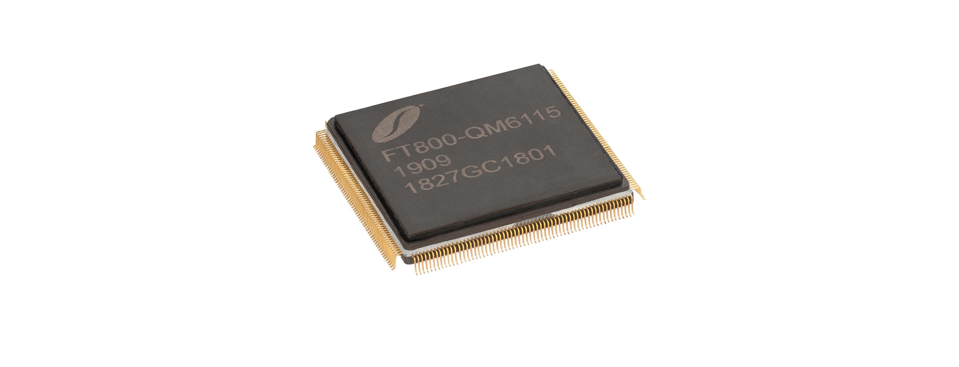
Typical package formats include
Custom tooling and lead forming is available where required.
Ceramic
CERDIP, CERPAC, CERQUAD, CQFP, Flatpack, JLCC, LCC, PGA, SIDEBRAZE
Plastic
PDIP, PLCC, SOIC/SSOP, SOJ, TQFP/PQFP, BGA
Specialist
Chip-on-board, Flex cable, Hybrid modules, TO can, Multichip Modules
Example packages
A selection of the package formats we manufacture and assemble
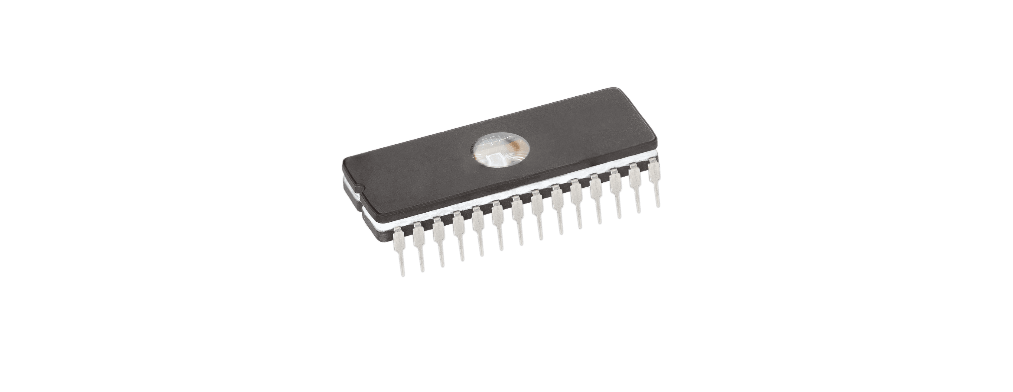
Windowed ceramic DIP
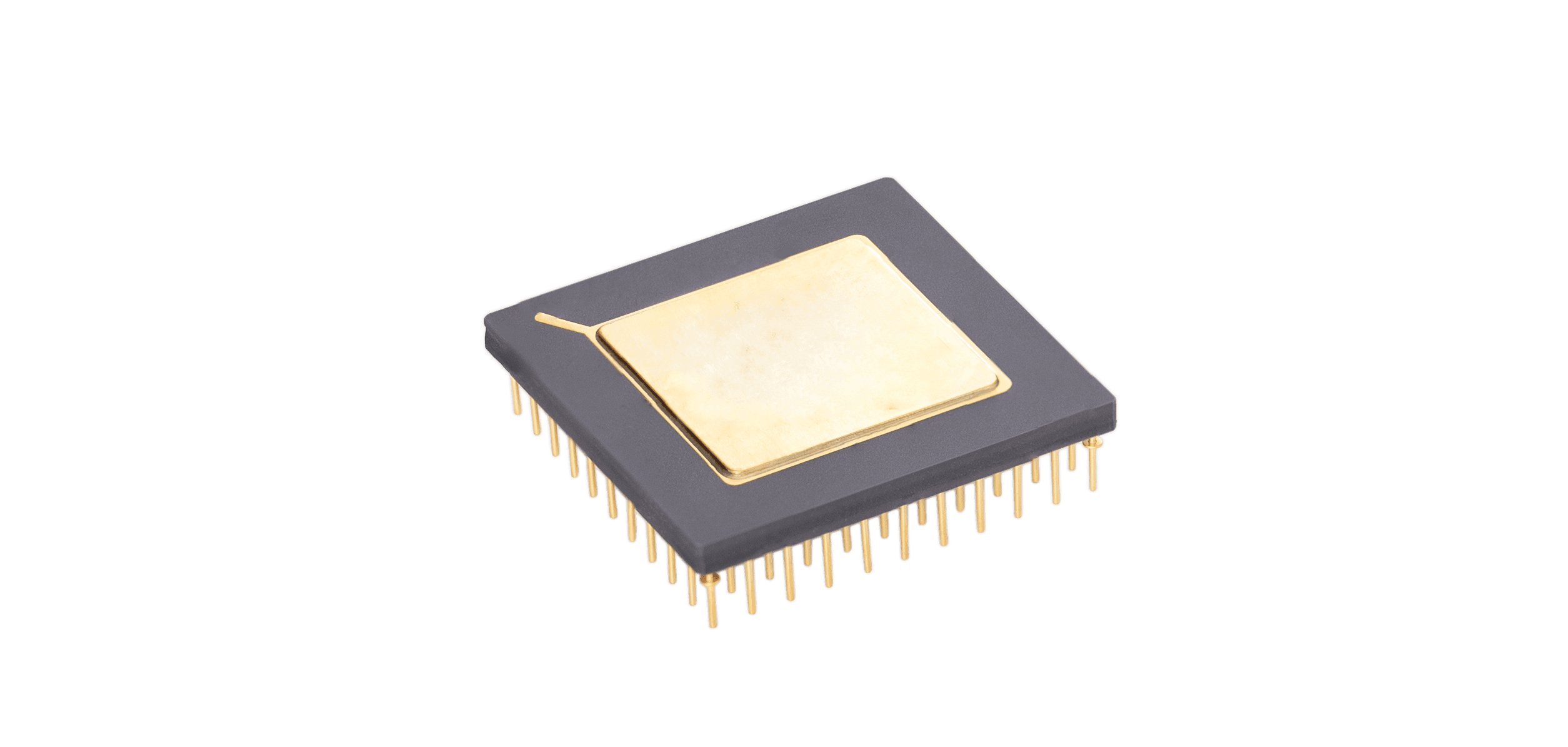
Ceramic pin grid array (PGA)
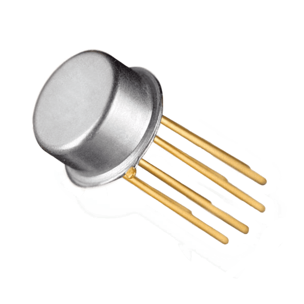
Metal can

TO-7 metal can
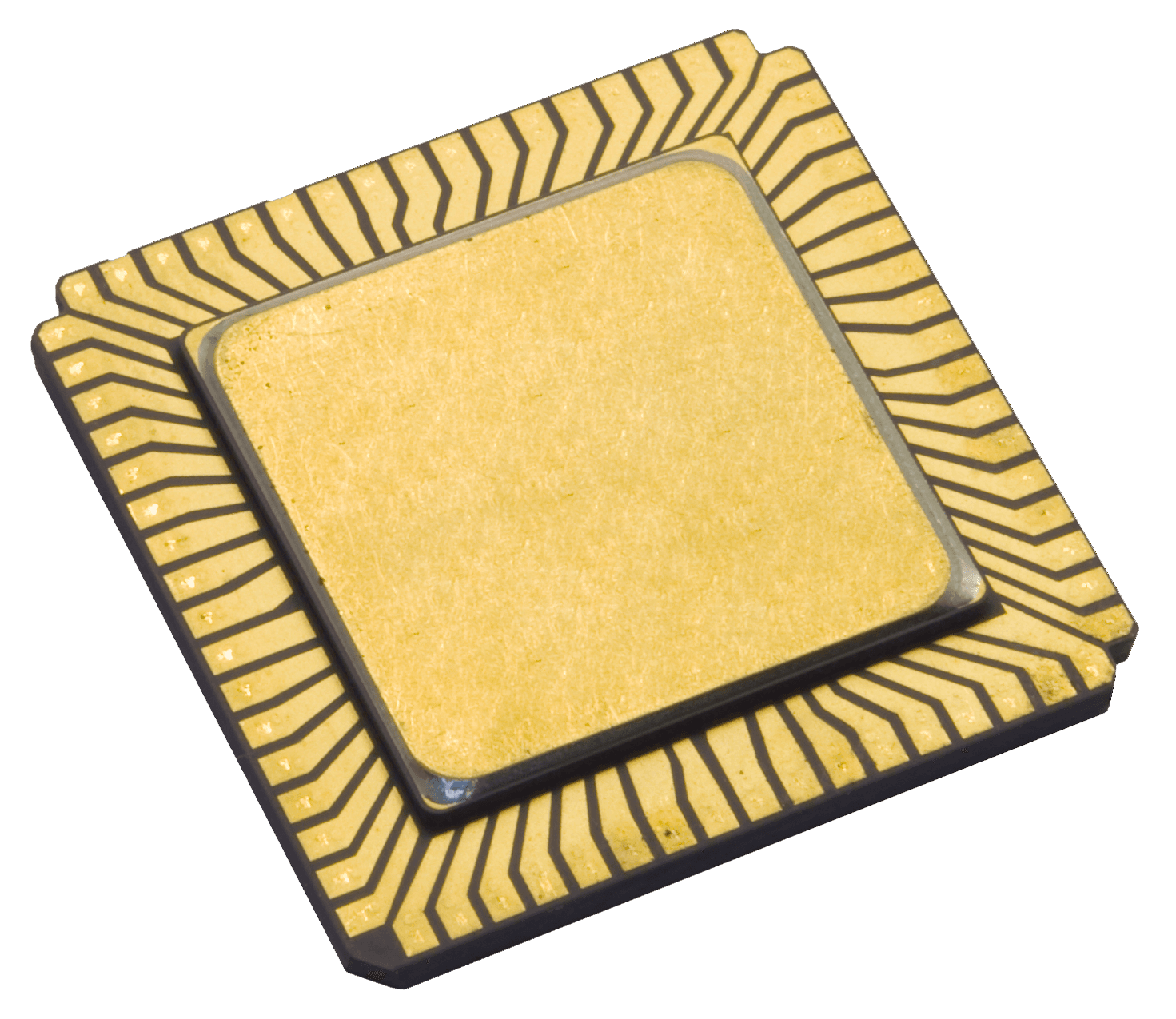
Micro package
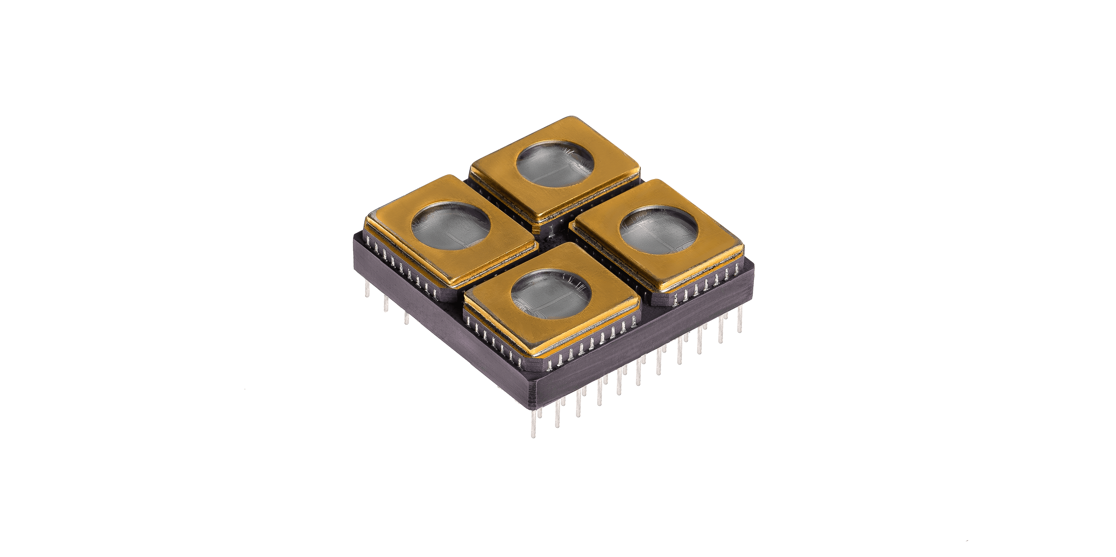
Custom package
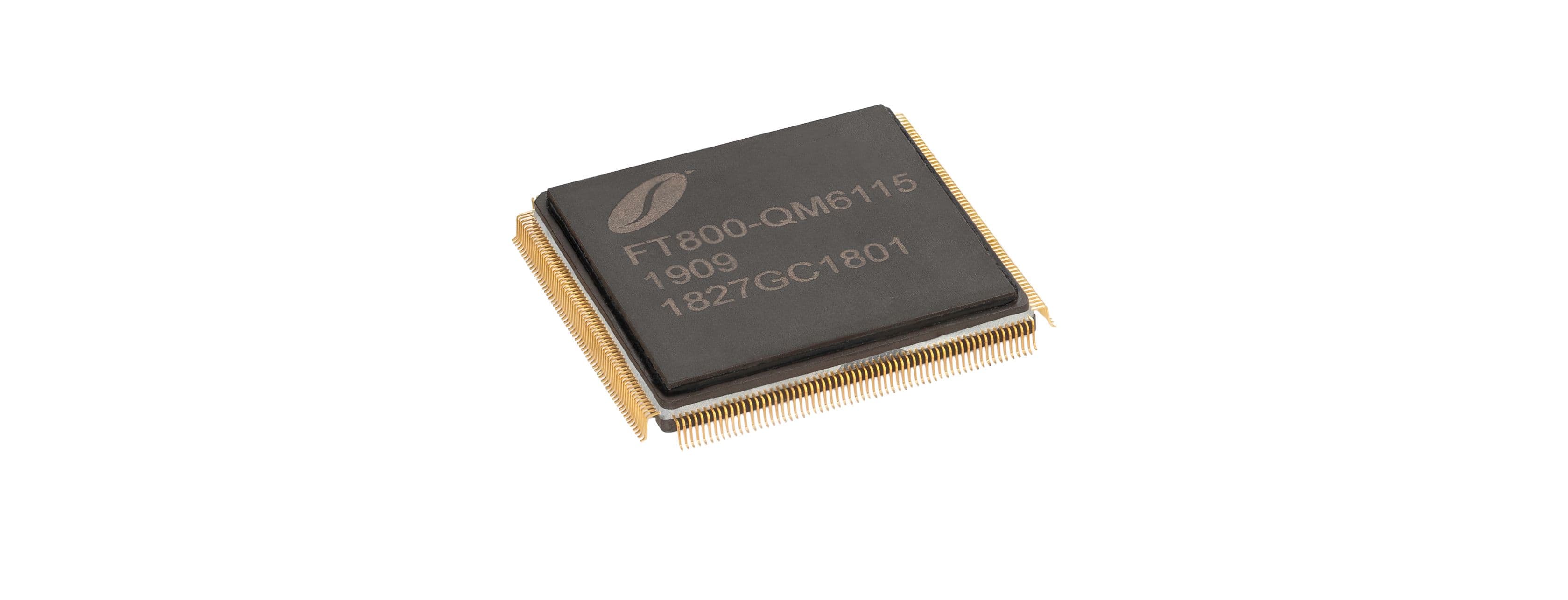
FPGA
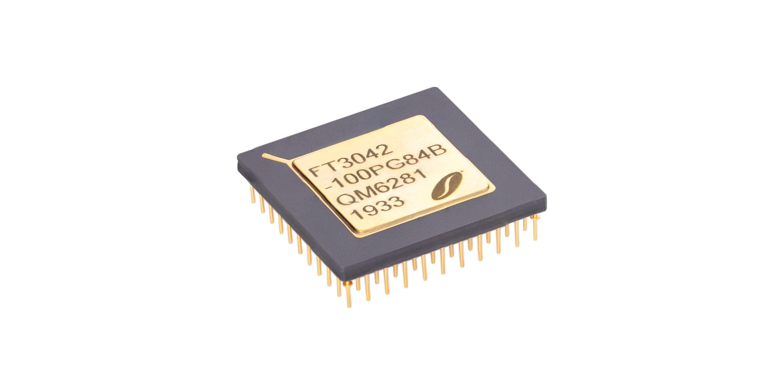
Ceramic PLCC
Frequently asked questions
What is IC packaging in relation to semiconductors?
IC packaging (Integrated Circuit packaging) refers to the final stage of semiconductor manufacturing, where the silicon die (the small chip that contains the integrated circuit) is enclosed in a protective casing. This packaging serves multiple purposes: 1. Protection: It shields the fragile silicon die from environmental damage, such as moisture, dust, and physical impacts. 2. Connectivity: The package provides a way to connect the chip to external circuits or systems via pins, pads, or other terminals. 3. Heat Dissipation: It helps in dissipating heat generated by the chip during operation. 4. Signal Transmission: Ensures efficient transmission of signals between the chip and the external environment. IC packaging is a critical step because it affects the performance, durability, and reliability of the semiconductor device in its intended application.
What types of packaging does Force Technologies offer?
IC packaging is available in various types, depending on factors such as the application, size, and complexity of the semiconductor. Force Technologies can assemble die into many different packages both plastic and ceramic such as: - DIP (Dual Inline Package): Traditional through-hole packages with pins on both sides. - QFP (Quad Flat Package): A surface-mount package with leads extending from all four sides. - BGA (Ball Grid Array): Uses an array of solder balls for connections underneath the chip. - Dual Inline Ceramic Package (CERDIP): Similar to the plastic DIP but made from high reliability ceramic. - Ceramic Leadless Chip Carrier (CLCC): A leadless package with contact pads on the bottom or sides. - Ceramic Quad Flat Package (CQFP): Similar to the plastic QFP but made from high reliability ceramic. - Custom footprints, lead styles and forming options. Please get in touch for more package options.
What are the five packaging criteria that should be considered?
When selecting an appropriate package for a semiconductor device, the following five key criteria should be considered: 1. Thermal Performance — Heat dissipation is critical to ensure the semiconductor operates within safe temperature limits. Ceramic packages are often preferred for high-power applications due to their excellent thermal conductivity. 2. Electrical Performance — The package must enable efficient signal transmission with minimal noise and signal loss. Ball Grid Array (BGA) packages are ideal for high-speed applications due to their reduced parasitics. 3. Mechanical Protection and Reliability — The package protects the die from physical damage and environmental factors like moisture, dust, and vibration. Hermetically sealed ceramic packages are often chosen for aerospace and military applications. 4. Size and Form Factor — The package must align with board layouts and the physical constraints of the application. Thin Small Outline Package (TSOP) is commonly used in memory chips where a low-profile and compact form factor is crucial. 5. Cost and Manufacturability — The package should balance performance and reliability with cost-effectiveness and ease of production. Plastic packages like QFP or QFN are popular for commercial electronics due to their low cost and ease of manufacture at high volumes. By carefully evaluating these criteria, you can select the most suitable IC package for the semiconductor’s intended application, balancing performance, reliability, and cost.
Ready to solve your packaging challenge?
Talk to us about your application requirements and we will identify the right package configuration to maintain supply and performance.